Organic Semiconductors
Since the beginning of the 21st century there has been an explosion of interest in a new class of materials, commonly known as Organic Semiconductors. The enormous progress in this field has been driven by the expectation to realize new applications, such as large area flexible light sources and displays, low-cost printed integrated circuits or plastic solar cells from these materials. Owing to the large efforts of both academic and industrial research laboratories, organic semiconductor devices have progressed rapidly and meanwhile lead to first commercial products incorporating organic semiconductors. Our group focuses on the fundamental physics behind this rapidly developing field of organic electronics.
Photophysics and light extraction in organic light-emitting diodes (OLEDs)
Like in their inorganic counterparts, the working principle of organic light-emitting diodes relies on the radiative recombination of injected electron–hole pairs in a solid, a process termed electroluminescence. In detail, however, the nature of electronic excitations and the structural peculiarities of organic molecular materials lead to marked differences concerning their opto-electronic properties. This holds true particularly for emitter materials in OLEDs, where spin-selection rules and molecular orientation are important parameters in determining their efficiency of converting electrical current into visible light. Our group is developing methods to analyze and improve OLED efficiency by combining experimental studies with numerical simulation. Recent research highlights have been the discovery of non-isotropic emitter orientation in molecular guest-host systems and its implementation in phosphorescent OLEDs as well as devices based on thermally activated delayed fluorescence (TADF).
Furthermore, spontaneous orientation polarization of molecules with permanent electrical dipoles modifies the energy landscape relevant for charge injection and transport. Recent research highlights have been the discovery of non-isotropic emitter orientation in molecular guest-host systems and its implementation in phosphorescent OLEDs as well as devices based on thermally activated delayed fluorescence.
Molecular donor/acceptor solar cells

Owing to the excitonic nature of photoexcitations in organic semiconductors, the working mechanism of organic solar cells relies on the donor-acceptor (D/A) concept enabling photoinduced charge transfer at the interface between two organic materials with suitable energylevel alignment. However, the introduction of such a heterojunction is accompanied by additional energy losses compared to an inorganic homojunction cell due to the presence of a charge-transfer (CT) state at the D/A interface. We are investigating the interrelation of film structure and morphology, electronic structure at interfaces as well as charge and exciton transport properties of a number of prototypical molecular D/A pairs and their performance in organic photovoltaic cells (OPVs). In particular, we develop quantitative methods to extract information on the mechanisms of charge generation and recombination in OPVs as well as their energy losses determining the overall power conversion efficiency.
Charge transport in semiconductors

Due to the intrinsically very low charge carrier density in organic semiconductors electrical conduction can only be enabled by generating excess carriers. To this end, different techniques are established, such as chemical doping or field-effect doping at the interface to a dielectric material. Such field-effect transistors are on the one hand the building blocks for logic circuits but on the other hand also serve as an important tool to study transport properties in a variety of materials.
In our work we study the growth behavior of organic heterostructures and their electronic properties, with particular focus on charge transfer (CT) occurring both in bulk mixtures as well as at sharp interfaces. Depending on the relative ionization potentials and electron affinities of the two partners, the degree of CT as well as its nature – ground vs. excited state – can be systematically varies. Applications range from interface doping in organic field-effect transistors (OFETs) to thermoelectric materials.
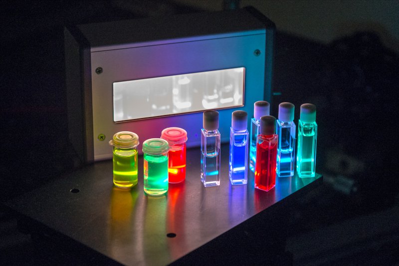
Semiconductor Nanocrystals

In recent years, colloidal semiconductor nanocrystals have become a viable alternative to purely organic opto-electronic materials. They can be processed as thin films from solution and are, thus, widely compatible with organic electronics. In our group, we study different types of opto-electronically active nanocrystals, ranging from visible light-emitting lead halide perovskite and InP quantum dots to infrared absorbers based on PbS. We modify their electronic properties and coupling via ligand exchange strategies, integrate them into organic optoelectronic devices and study their fundamental device physics.
Numerical Simulations

With the increase of computational performance numerical simulations of organic semiconductors are nowadays no longer limited to high performance clusters. Within this development, density functional theory (DFT) and molecular dynamics (MD) simulations became a frequently used tool in our work group. The calculation of molecular quantities like the molecular dipole moment or the transition dipole moment that is responsible light emission are of crucial importance for the interpretation of experimental results. Additionally, we are trying to develop ab initio methods combining both aforementioned techniques in order to predict thin film morphologies.
Further Reading
- Organic Semiconductors, W. Brütting, in: R.G. Lerner, G.L. Triggs (Hrsg.): Encyclopedia of Physics, Wiley-VCH (2005) 1866-1876 [ PDF]
- Grundlagen der organischen Halbleiter, W. Brütting, W. Rieß, Physik Journal 7(5) (2008) 33-38. [ PDF]
- More light from OLEDs, Europhysics News 42 (4) (2011) 20-24. [ PDF]
- Physics of Organic Semiconductors 2nd Edition, W. Brütting, C. Adachi, Wiley-VCH (2012). [ Wiley-VCH]
- Mehr Licht durch orientierte Farbstoffmoleküle, T.D. Schmidt, T. Lampe, W. Brütting, Nachrichten aus der Chemie 64 (5) (2016) 514-518. [ Link]
- Organic LEDs and Solar Cells United, W. Brütting, Nature Materials N&V, 18, 232-233 (2019). [ PDF]
Collaborative Research Projects
- European Union Horizon 2020 Marie-Sklodowska-Curie Innovative Training Network - "TADFlife - Using the smart matrix approach to enhance TADF-OLED efficiency and lifetime" [ Web-Link]
- German Ministry for Education and Research (BMBF) - "ELQ-LED: Erforschung von Quanten-Materialien - Neue Wege zur Realisierung innovativer optoelektronischer Bauteile" [ Web-Link]
- Bavarian State Ministry of Science, Research and the Arts - “Solar Technologies go Hybrid (SolTech)“ [ Web-Link]
- German Research Foundation (DFG), Priority Program SPP 2196 – “Perovskite semiconductors: From fundamental properties to devices” [ Web-Link]
Contact Person
Contact information:
Address:
Experimentalphysik IV
Institut für Physik
Universität Augsburg
Universitätsstr. 1
86159 Augsburg
Phone: +49 821 598 -3402 (Office)
Fax: +49 821 598 -3425
E-Mail: sekretariat_ep4@physik.uni-augsburg.de (Office)
Building: R
