Transmission Electron Microscope (TEM)
The transmission electron microscope is one of the most expensive and complex instruments in the lab. Basically, it is build similar to an optical transilluminated light microscope. Instead of light, electrons are used and instead of glass lenses, electromagnetic lenses and deflectors must be used to focus and manipulate the electron beam. The electrons used in a TEM have a wavelength in the picometer range, while visible light has a wavelength in the range of several hundred nanometers. Since the resolution of an optical instrument depends strongly on the wavelength of the used probe, the resolution of a TEM is several orders higher than that of a light microscope. To keep it short, the TEM is capable to resolve individual atoms, the resolution limit is around 60pm.
One of our TEMs and a schematic and simplified setup is shown in fig. 1.
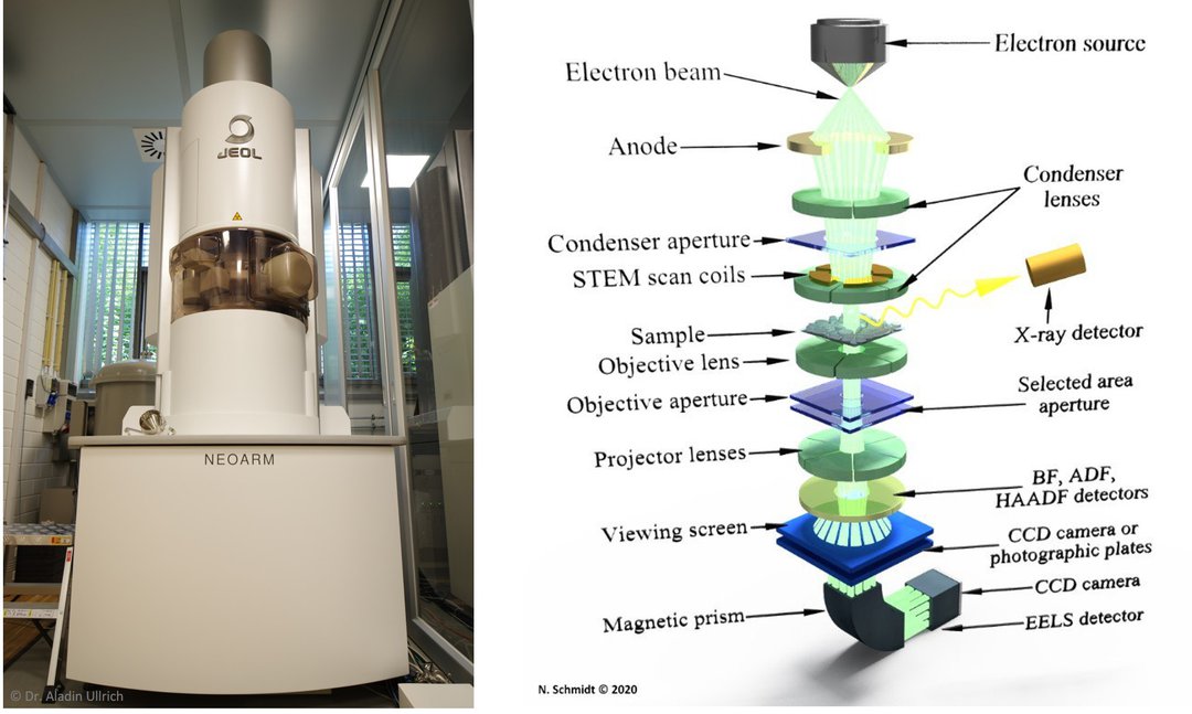
Fig. 1: left: one of our TEMs. Right: schematic setup of a TEM.
To image the sample, the electrons are accelerated to an energy of 200 – 300 keV and targeted to the sample. The transmitted electrons are detected and a magnified image of the sample is generated. To get a transmitted signal, the sample must be quite thin. Thin means below 100nm, best would be < 50nm. Such samples are quite complicated to prepare. Fig. 2 shows the principle of the preparation of a cross-section TEM sample of a layered structure on a substrate. Such a preparation may take up to two days.
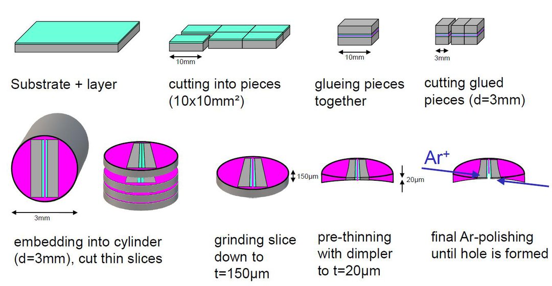
Fig. 2: Preparation of a cross-section sample from a thin layer.
A modern TEM is capable to reach sub-Angström resolution (<100pm). Fig. 3 shows PbS nanoparticles with a size of 5 nm on a carbon support film. A careful look at the image reveals small white dots in between the particles. This are individual Pb atoms, released from the particles and lounging around on the carbon substrate.
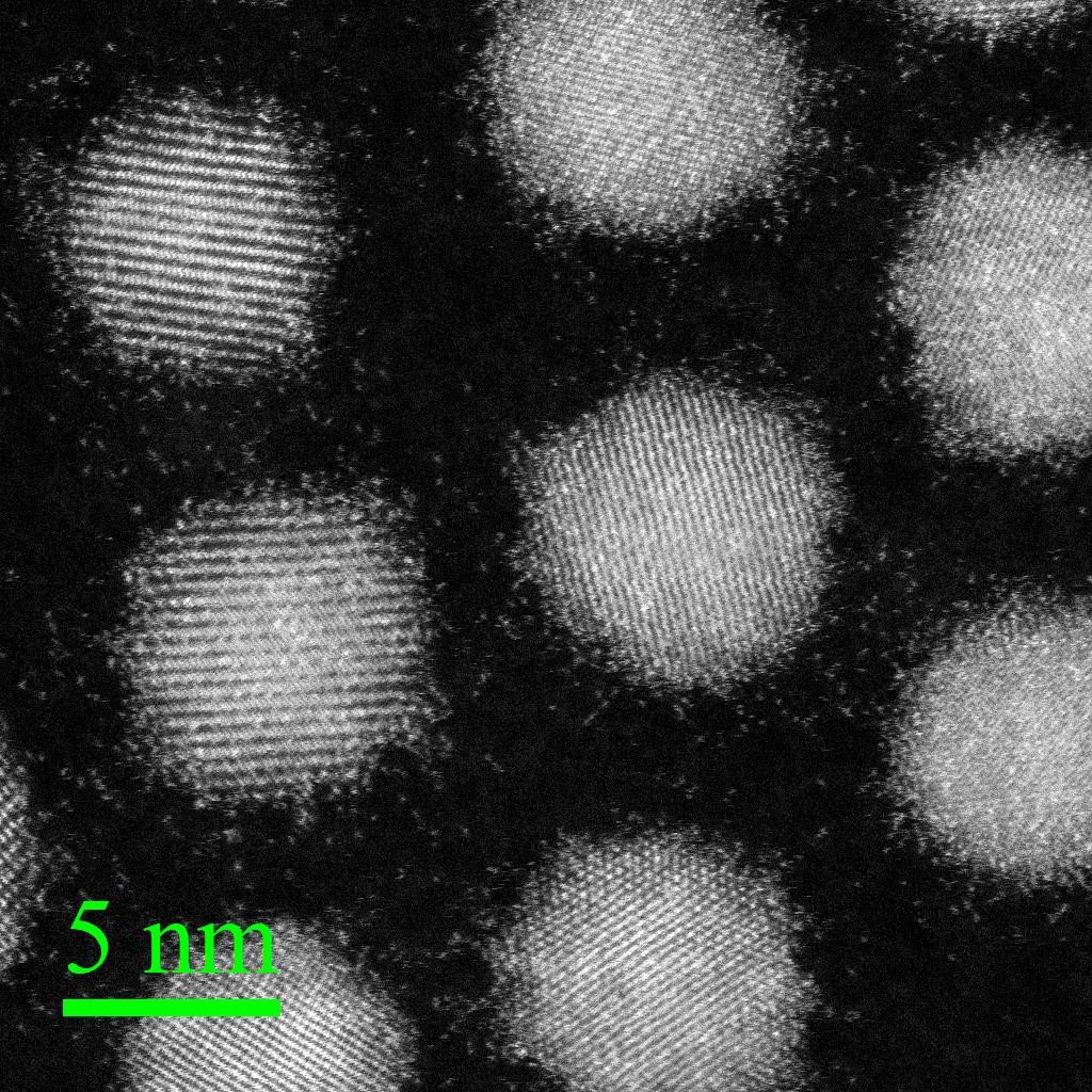
Fig. 3: PbS nanoparticles with individual lead atoms in between them.
Beyond imaging on atomic scale, a wide spectrum of other information is accessible. The high-energy electron beam excites the atoms in the sample to emit characteristic x-rays. Theses x-rays can be detected and the elemental composition of the sample can be investigated. With a focussed beam rastering over the sample, an atomic resolved elemental map can be generated as shown in fig. 4 for a crystalline SrTiO3 sample, oriented along the <100> zone axis.
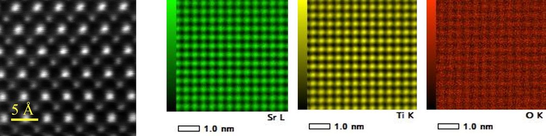
Fig 4: Left: High-angle annular dark filed image of SrTiO3. Brighter spots: Sr atoms, darker spots: Ti atoms. Oxygen atoms are not visible. Right: atomic resolved elemental maps of the elements.
Besides the elemental composition, so called “chemical maps” can be generated by measuring the energy loss of the electrons that have passed the sample. In this signal, besides the elemental information there is also information about the electronic structure of the atoms, i.e. for example the oxidation state can be deduced. Fig. 5 shows a chemical map of a manganese ferrite core-shell nanoparticle. The core contains Fe2+, while the iron in the shell is in the 3+ state proved by a shift of the Fe L3 edge in the EEL spectra.
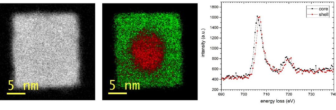
Fig. 5: Chemical map of iron oxide core-shell nanoparticles: the shell of the particle contains Fe3+, while the core consists of Fe2+. This is manifested by a shift of the Fe L3 edge of about 1 eV, represented by the red and green colour, respectively (center). The HAADF image (left) does not show a visible core-shell contrast.
At our chair we are investigating magnetic thin layers. With a TEM it is also possible to visualize magnetic domains and domain walls. To observe the sample in a field-free condition, the objective lens of the instrument must be switched off since the sample is placed in the center of this lens. This is called the “Lorentz-Mode” since now the electrons are influenced by the Lorentz force within the sample. For imaging, a so called “Lorentz Lens” is used: the field from this lens does not reach the sample region, but it also does not reach atomic resolution. Fig. 6a shows a typical Lorentz image with a maze-like domain wall structure. From a focus series a so called “induction map” can be created. This visualizes the direction of the magnetization. The objective lens can now be used to generate a magnetic field and observe the response of the sample. In this sample, magnetic vortices (skyrmions) can be observed under a small magnetic field as shown in fig. 6b.
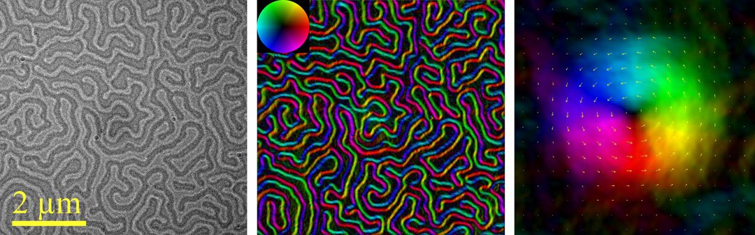
Fig. 6: Left: Lorentz TEM of a sample with a maze-like domain wall structure. Center: induction map. Right: same sample with applied magnetic field (out of plane direction) of 30mT shows skyrmions (diameter approx. 200nm).
Since conventional TEM images are projections of a 3D sample on a 2D image, the 3D structure of the samples are not accessible from a single image. To reveal the 3D structure of a sample, tomographic techniques can be applied. Fig. 7 shows a metal organic framework (MOF) crystal with in-situ grown Pt nanoparticles (2nm). From a series of images taken at tilt angles ranging from -79 to +68° with respect to the electron beam, a 3D reconstruction of the MOF crystal can be generated. From this reconstruction, it becomes clear that the Pt nanoparticles are situated on the surface of the crystal and not in its volume.
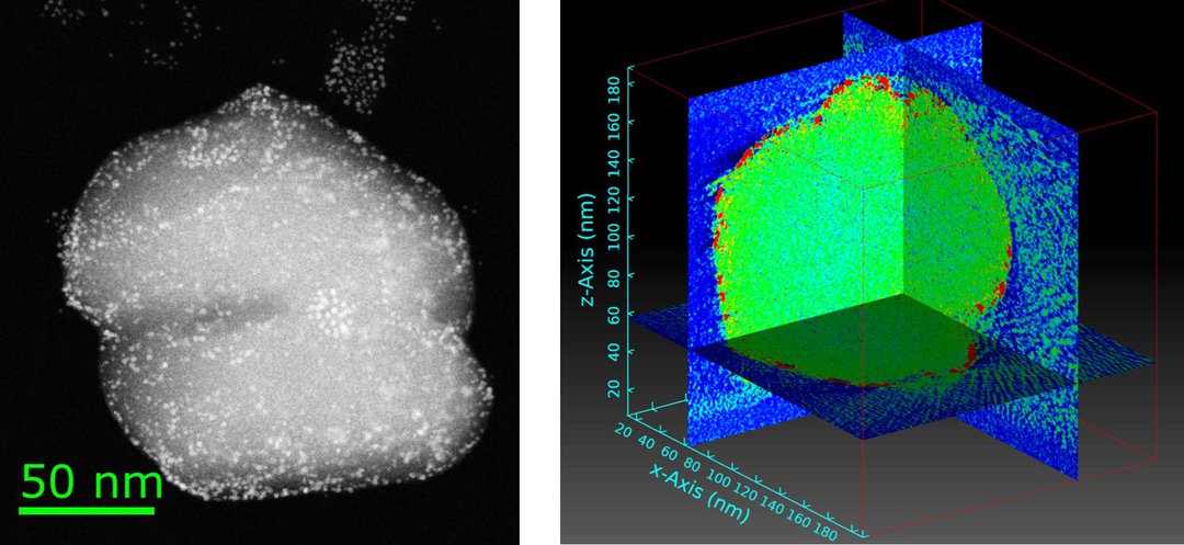
Fig 7: Metal organic framework (MOF) with Pt nanoparticles. Left: HAADF-STEM-image of a MOF-crystal with Pt-nanoparticles (d = ca. 2nm). Right: cut through a 3D-reconstruction of the same MOF, generated from 140 images (tilt range: -79 to 69°). Green: MOF; red: Pt nanoparticles. The reconstruction reveals the presence of the Pt nanoparticles only at the surface oft he MOF, not in the inner regions.
Contact person: Dr. Aladin Ullrich